Products
Deposition Systems
Samco’s thin-film deposition systems deliver high-quality dielectric film growth and passivation layers for compound semiconductors, silicon substrates, and advanced electronic devices. Engineered for uniform step coverage and stress control, our portfolio spans atomic-layer deposition up to thick films of tens of micrometers. Built to bridge the gap between Lab and Fab, Samco systems enable seamless scaling from basic research and laboratory development to full-scale volume manufacturing.
-
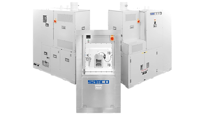
ALD Systems
Samco’s atomic layer deposition (ALD) systems deliver highly uniform, pinhole-free dielectric and functional thin films for compound semiconductors, silicon substrates, and advanced electronic devices. Driven by sequential, self-limiting surface reactions, our thermal and plasma-enhanced ALD technologies provide precise atomic-scale thickness control and exceptional step coverage over extreme aspect ratio structures. Built to bridge the gap between Lab and Fab, Samco ALD platforms enable reproducible process scaling from fundamental university research to automated volume production.
-
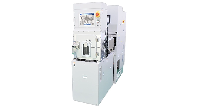
PECVD Systems
Samco’s plasma enhanced chemical vapor deposition (PECVD) systems utilize radio frequency (RF) generated plasma to form high-density dielectric and passivation films at reduced substrate temperatures. Designed to optimize film stoichiometry and physical stress, our PECVD equipment enables uniform deposition of silicon oxide (SiO2), silicon nitride (SiN), and silicon oxynitride (SiON). Built to bridge the gap between Lab and Fab, Samco PECVD platforms deliver stable, repeatable film growth across compound semiconductors, silicon devices, and advanced electronic devices.
-
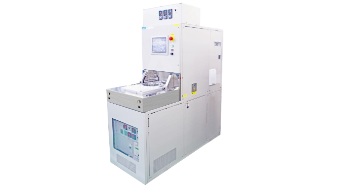
LSCVD Systems
Engineered for low-temperature deposition, Samco’s Liquid Source Chemical Vapor Deposition (LSCVD) system processes silicon dioxide (SiO2) and silicon nitride (SiN) films using liquid precursors like TEOS and SN-2. By vaporizing liquid precursors, the system deposits high-quality dielectric and passivation layers without high thermal processing—protecting heat-sensitive substrates (such as compound semiconductors, flexible polymers, and microelectronics) from thermal stress and degradation.Equipped with a specialized liquid delivery system, the LSCVD ensures uniform film thickness, exceptional step coverage, and reliable process repeatability. With its compact footprint, it delivers a versatile, dependable solution for advanced R&D and specialized production across "Lab and Fab."
Etching Systems
Samco’s dry etching systems utilize radio frequency (RF) generated plasma to achieve high-precision micro-fabrication for compound semiconductors, silicon substrates, and advanced electronic devices. By harnessing the synergistic effects of active radicals and physical ions within the plasma, our equipment delivers highly anisotropic profiles with fine line-width control. Engineered to bridge the gap between Lab and Fab, Samco etching platforms enable seamless process scaling from university research to commercial volume manufacturing.
-
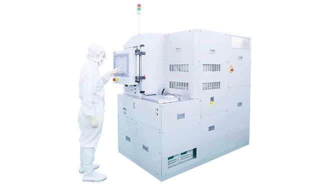
ALE Systems
As next-generation compound semiconductor devices such as GaN HEMTs, SiC power transistors, and high-density 2D electronics continue to scale down, conventional continuous Inductively Coupled Plasma (ICP) etching encounters critical physical limitations. Standard plasma processes often introduce crystal lattice degradation, surface roughness, and uncontrolled over-etching due to high-energy ion bombardment and continuous chemical exposure. Samco’s Atomic Layer Etching (ALE) technology overcomes these physical constraints by decoupling the etching process into sequential, self-limiting reaction steps. By strictly separating chemical surface modification from reaction product desorption, our systems deliver sub-nanometer depth precision, preserve underlying crystal integrity, and ensure complete immunity to micro-loading across varying pattern densities, bridging the gap from advanced laboratory research to high-volume manufacturing.
-
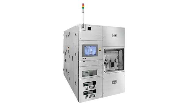
ICP Etching Systems
Samco’s Inductively Coupled Plasma (ICP) etching systems combine independent high-density plasma generation and directional ion acceleration to deliver fine-pattern micro-fabrication for compound semiconductors, silicon substrates, and advanced electronic devices. By decoupling plasma density from substrate bias, our ICP platforms achieve high etching rates, smooth sidewall morphology, and excellent profile control over high-aspect-ratio structures. Built to bridge the gap between Lab and Fab, Samco ICP etching systems enable predictable process scaling from initial device research to automated volume production.
-
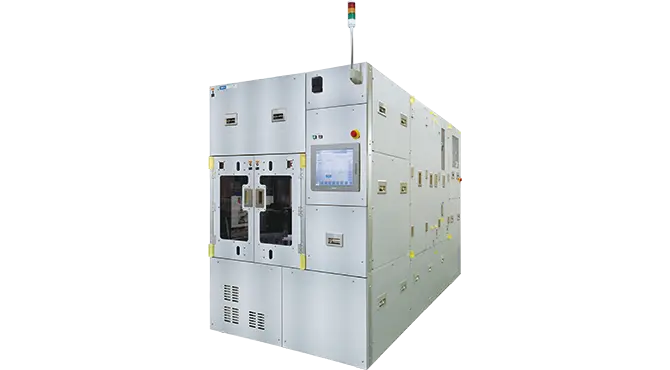
Si DRIE Systems
Samco’s Silicon Deep Reactive Ion Etching (Si DRIE) systems utilize high-density plasma technologies to achieve fast, high-aspect-ratio micro-fabrication in silicon substrates. Equipped with high-precision gas switching networks, 5 kW high-power RF sources, and temperature-controlled electrostatic chucks (ESC), our equipment enables fast, alternating etch-passivation cycling using the Bosch Process. Built to deliver exceptional process stability, Samco Si DRIE platforms provide repeatable silicon processing for MEMS, TSV, and advanced packaging applications.
-
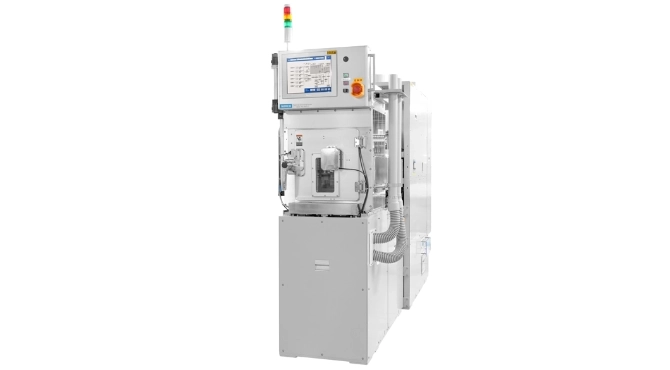
CCP-RIE Systems
Samco’s Capacitively Coupled Plasma Reactive Ion Etching (CCP-RIE) systems provide stable dry etching solutions for dielectric thin films, fluorinated polymers, and surface modification processes. Utilizing parallel-plate electrode configurations, our CCP platforms generate uniform, low-density plasma across large substrate areas. Designed to meet versatile R&D and production requirements, Samco CCP-RIE systems offer broad operational windows for academic laboratories and semiconductor manufacturing facilities alike.
Surface Treatment Systems
Samco’s surface treatment systems employ atmospheric and vacuum plasma technologies to perform dry cleaning, surface activation, and surface modification on substrates and microscopic components. By selectively modifying surface energy and removing organic residues without damaging underlying fine structures, our platforms prepare surfaces for subsequent processes such as thin-film deposition, bonding, and encapsulation. Designed to bridge the gap between Lab and Fab, Samco systems enable flexible process adaptation from initial laboratory research to continuous automated production.
-
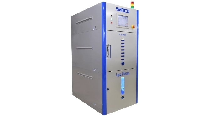
Aqua Plasma® Cleaners
Aqua Plasma® cleaners is a plasma treatment system that uses water vapor (H₂O) as a reactive gas. It performs metal oxide reduction, direct bonding, surface hydrophilization, and organic contaminant decomposition. Designed to support both fundamental research and industrial manufacturing lines, Samco Aqua Plasma® cleaners ensure consistent process repeatability for packaging and device fabrication workflows.
-
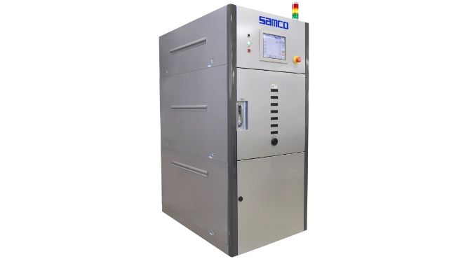
Plasma Cleaners
Samco’s Plasma Cleaners utilize controlled, low-temperature gas discharge plasma to achieve thorough surface cleaning, organic residue removal, and surface energy alteration across electronic components, compound semiconductors, and optical devices. Operating with oxygen (O2), argon (Ar), or mixed gas configurations, these systems break down molecular-level organic contaminants and tailor substrate surface chemistry without altering bulk material properties. Designed to support both fundamental research and industrial manufacturing lines, Samco Plasma Cleaners ensure consistent process repeatability for packaging and device fabrication workflows.
-
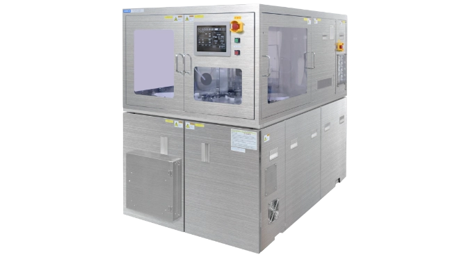
UV Ozone Cleaners
Samco’s UV-Ozone Cleaners utilize a controlled synergistic combination of short-wavelength ultraviolet (UV) light, high-concentration ozone (O3), and stage heating to perform high-precision dry surface treatment across semiconductor, display, and electronic device manufacturing lines. Operating under ambient pressure without reactive ionic species, these systems break down molecular-level organic contaminants from silicon wafers, compound semiconductor substrates, glass, and metallic electrodes without causing physical plasma damage or electrostatic charge buildup. Designed to support both fundamental laboratory R&D and high-throughput production environments, Samco UV-Ozone Cleaners deliver highly repeatable surface activation and wettability enhancement.
Explore Solutions via Processes
Our Strengths
-
Engineering Excellence Meeting Diverse Global Needs
Samco leverages industry-leading expertise in plasma process technology. Our semiconductor manufacturing equipment enables uniform thin-film deposition at low temperatures and high-precision processing of compound semiconductors, providing versatile solutions tailored to diverse global industry requirements.
-
Support
Beyond product sales, Samco provides comprehensive after-sales support and maintenance. We ensure the continued reliability of your equipment through proactive inspections and responsive troubleshooting. Should you have any questions or require assistance regarding our systems, please contact our dedicated user support team.

