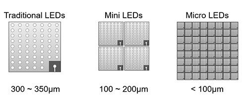
Over the last year, next-generation microLED displays have begun to surpass the conventional liquid crystal and organic EL displays, and are starting to attract more and more attention from industry leaders. While the exact definition of microLED hasnʼt been decided by the display industry, "microLED" typically refers to an LED chip with side lengths of 100 microns down to several microns. LED chips in the 100 to 200 micron range, such as those used in Samsungʼs famous The Wall, are typically referred to as "miniLEDs."

Like traditional LEDs, microLED chips have rows and columns of semiconductor structures which emit a combination of red, green or blue light to produce a wide range of colors. The materials used as the semiconductor elements in an LED chip determine their color. The most commonly used materials are InGaN for green, blue and white LEDs and AlGaInP for red, orange and yellow LEDs. Gallium nitride (GaN) is an excellent semiconductor material for LEDs because of its direct bandgap, high electron Samco's Solution for Micro LEDs mobility and thermal conductivity. By mixing GaN with a small percentage of indium nitride (InN) it is possible to tune the band gap to efficiently emit green, blue or white light.
At submillimeter sizes, microLED chips can be fabricated and put into arrays to be used as individual RGB pixels in TV and smartphone displays with higher brightness and lower power consumption than ever before. MicroLEDs also have near perfect black levels which, when paired with their brightness, means an excellent contrast ratio making them ideal for high dynamic range (HDR), augment reality (AR) displays and heads-up displays (HUD). Of course, with new technological breakthroughs there are always some hurdles to overcome. For microLED technology the largest challenge is finding cost effective methods to produce displays with millions of microLEDs. Another critical factor when an LED shrinks is the defect density. It has been demonstrated that the impact of sidewall defects, generated during the etching process, on device performance cannot be ignored for LEDs at the micro-level size. This is due to the increased importance of Shockley-Read-Hall recombination as the size of GaN-based LEDs shrink. On the other hand, microLEDs with perfectly fabricated sidewalls actually see an increase in efficiency as they decrease in size.
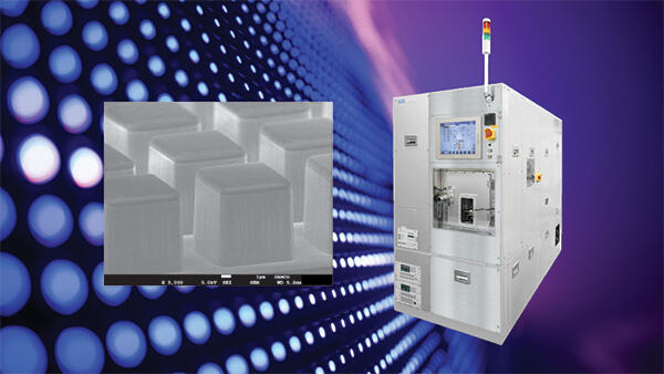
The challenge of GaN etching is that the tight crystalline bond strengths in group III nitride materials are what gives them attractively wide bandgaps, but it also makes the material chemically inert and difficult to etch. In particular, there is difficulty in obtaining smooth etched sidewalls because of the inherent generation of damage inducing ions in dry etching processes.6 To address this, Samco uses an inductively coupled plasma reactive ion etching (ICP-RIE) process with chlorine-chemistry which can achieve high etch rates for mesa etching while maintaining smooth and highly anisotropic sidewalls.
To continue, please submit the form.


