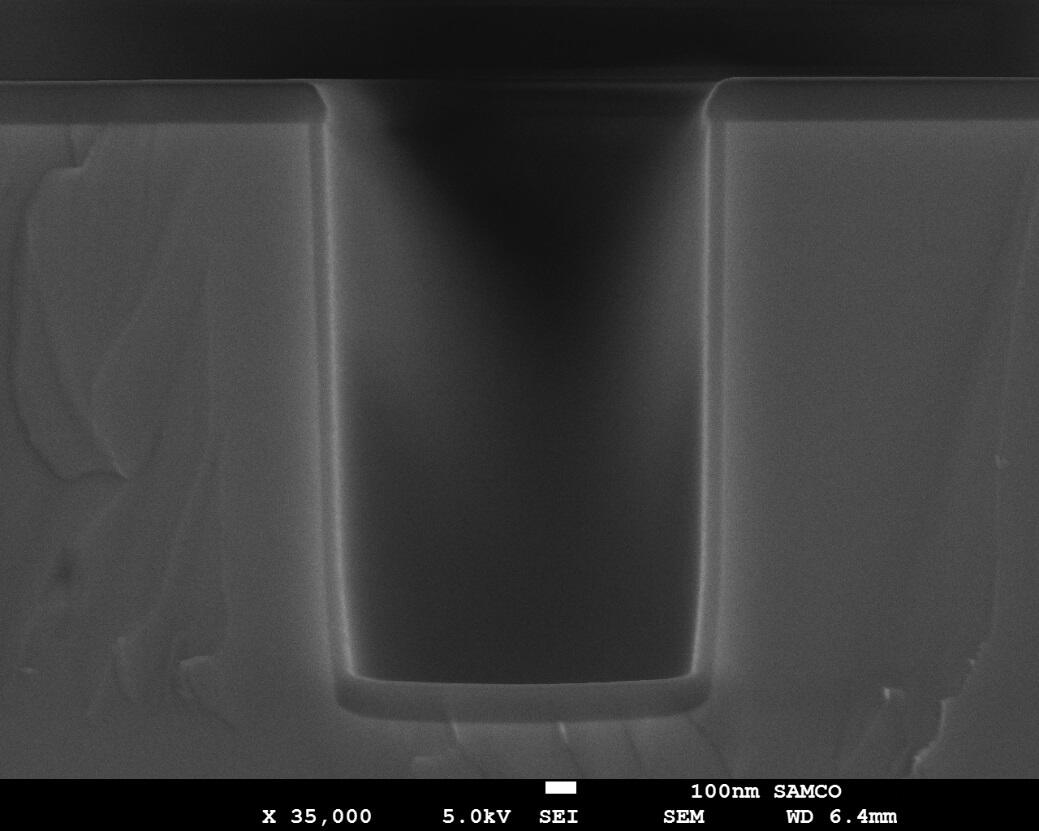
Compared to the mainstream semiconductor Si, the wide bandgap semiconductor 4H-SiC has excellent material qualities including higher electrical breakdown strength and higher thermal conductivity.Therefore, 4H-SiC has been studied in recent years as a new material to improve miniaturization and energy saving in power devices. Currently, it is being developed not only for device fabrication but also for practical
applications in the automotive and power supply industries. SiC MOSFETs (Metal Oxide Semiconductor Field Effect Transistors) are one example of commonly used 4H-SiC power devices that surpass Si power devices in terms of high voltage endurance, low on-resistance, and high-speed switching. Trench type SiC MOSFETs are being developed and have shown that they are capable of achieving a reduced on-resistance, which is highly demanded in current devices. We have been developing a trench etching process using plasma dry etching and deposition of the gate insulator using ALD (Atomic Layer Deposition) and PECVD (Plasma Enhanced Chemical Vapor Deposition). These processes are required for manufacturing trench type SiC MOSFETs.
In this paper, we will highlight the SiC trench etching and gate insulator deposition results.
To continue, please submit the form.


