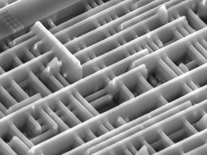
5 Layer Al Wiring
Defect analysis of exposed 5-layer Al wiring by RIE plasma etching system.
The removal of the silicon nitride film (SiN) as a passivation film and the silicon oxide film (SiO₂) as an interlayer insulator has been achieved while leaving the Al wiring.
In addition to the above, we have performed processes to suppress polyimide residues, removal of low-k organic silicon interlayer insulation, sequential removal of multilayer Al interconnects, high selectivity processes for Poly-Si and TiN, exposure of tungsten plugs, and resin opening (decapping). In addition, we have a lineup of equipment for defect analysis, including a desktop type small RIE system, a parallel flat plate type RIE system for ø300mm, and an ICP etching system equipped with an electrostatic chuck (ESC) and a cooling mechanism by He. We can propose a wide range of solutions and optimal equipment according to customer needs.


