The loading effect and the microloading effect are common phenomena observed not only in deep Si etching but also in conventional Reactive Ion Etching (RIE), and are a barrier to achieving a depth uniformity in etching processes. These two effects strongly appear in the Bosch process (silicon deep reactive ion etching), which is mainly composed of fluorine radical etching. The loading effect is caused by the difference in the consumption rate of fluorine radicals as the etchants. The microloading effect is caused by the difference in the numbers of fluorine radicals transported in narrow spaces (Ex. trenches and holes with a high aspect ratio). Samco processes suppress these two effects and can control the etching depth and achieve excellent uniformity. In addition, the method of microloading effect suppressing can be applied to flattened bottom surface process, which we call the "flat bottom process".
■Loading Effect
The loading effect is a phenomenon in which the etch rate change depending on Si aperture (unmasked area) ratios. On the surface of Si, the fluorine radicals are consumed and the by-product, SiF4, is increased. Therefore, a larger aperture ratio of Si area has less fluorine radicals, and the etching rate becomes lower. A typical example is that bare Si wafers show slower etch rates at the center where the Si is exposed to a higher density than at the outer periphery.
Figure 1 shows the etching rate dependency on the aperture ratio of an ø8 inch Si wafer. The etch rate is 40 μm / min at an aperture ratio of 1% and goes to 15 μm / min when the aperture ratio is above 40%.
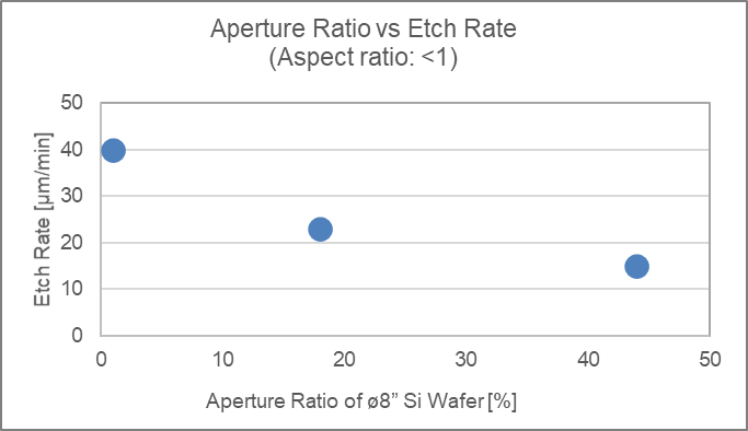
Fig. 1: Aperture ratio dependency of Si trench etch rate (ø8 inch wafer)
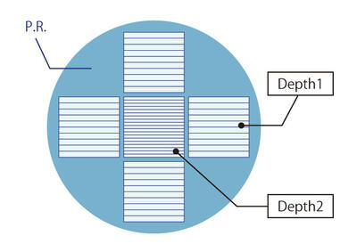
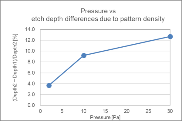
The loading effect is most noticeable when the sample includes both sparse and dense mask patterns, as shown in Figure 2a. In this case, there are two ways of tackling the loading effect issue. The first is to reduce the process pressure and promote gas diffusion. Figure 2b shows the relationship between the process pressure and the difference in depth between Depth 1 (sparse mask pattern) and Depth 2 (dense mask pattern) in Figure 2a. You can see that at lower process pressure, there is a smaller difference in depth. However, by lowering the pressure, the etch rate is also decreased. The second method is to create a dummy pattern on the wafer to reduce the density difference of the mask pattern.
(a) Example of sparse and dense mask pattern
(b) Pressure vs etch depth differences due to pattern density
Fig. 2: Pressure vs etch depth differences due to pattern density
■Microloading Effect
The microloading effect is a phenomenon in which fewer fluorine radicals transport the bottom of narrow gaps, causing the etch rate to decrease depending on pattern width. This phenomenon is also known as the RIE lag effect or ARDE (aspect ratio dependent etching). Figure 3 is an SEM image of the microloading effect after Si deep reactive ion etching.
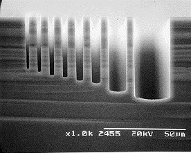
Fig. 3: SEM image of the microloading effect
When a pattern has a wide opening (right side of Fig. 3), fluorine radicals transport the bottom of trenches and holes easily, and can be processed at a high Si etch rate. However, when the pattern opening narrows (left side of Fig. 3), the etch rate gradually decreases with the number of fluorine radicals that are able to transport the bottom of the trench or hole. On the other hand, when processing pillar structures, the pattern width has little effect on the etch rate because the flow of fluorine radicals is not obstructed. In the case of trench and hole etching, it is more difficult for fluorine radicals to transport the bottom of patterns with high aspect ratios. This tendency is especially noticeable when etching holes, because radicals are obstructed independently of the direction from which they enter. This is unlike trenches, where radicals are less restricted when moving along the trench line. The rounded bottom seen in Fig. 3 is also due to side walls blocking the flow of fluorine radicals, which increases the ratio of radicals etching the center of the pattern.
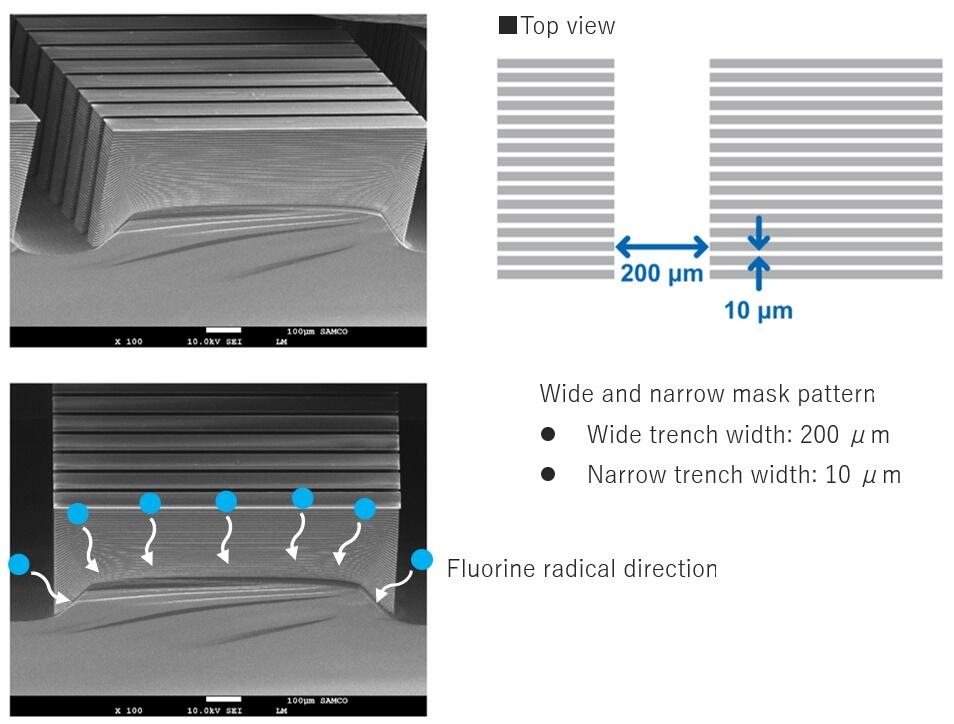 Fig. 4: SEM image of narrow and wide trench etch
Figure 4 shows SEM images of a narrow trench (10 μm) and a wide trench (200 μm) connecting. When a wide trench pattern intersects a narrow trench pattern, fluorine radicals are able to flow from the wider area, increasing the etch rate thus achieving a higher aspect ratio than would be the case for a pattern of only narrow trenches. However, due to the flow of fluorine radicals from the wider area, scallops will form diagonally instead of horizontally. Comb-shaped MEMS devices are another example of patterns with a mixture of narrow and wide trenches. For comb-shaped MEMS devices on SOI (Silicon on Insulator) wafers, even with relatively high aspect ratios, it is possible to etch through to the insulating layer.
■Method for Suppressing Microloading Effect
Figure 5 compares the normal Bosch process with Samco's method for suppressing the microloading effect. The normal Bosch process etches all of the passivation film on the bottom of the trench. Then, in the Si etching step, the etch rate is higher at the bottom of the wider pattern, especially in the center where fluorine radicals are more easily transported. As a result, depth uniformity worsens.
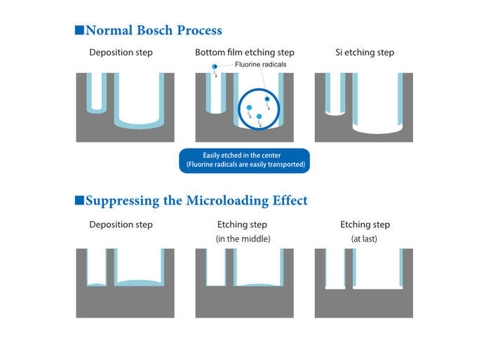
Fig. 5: Diagram of the Samco process to suppress the microloading effect
To suppress the microloading effect, some process conditions, such as the pressure during the deposition step, must be adjusted. In the etch step, the difference in the thickness of the deposited film and the difference in the etch rate are balanced and cancel each other out, achieving total depth uniformity. The microloading effect can then be suppressed by optimizing the duration of film deposition and etching for all pattern widths. Figure 6 shows the result of adjusting the process conditions to control the microloading effect.

Fig. 6: SEM images of control of the microloading effect
■Flat-Bottom Process
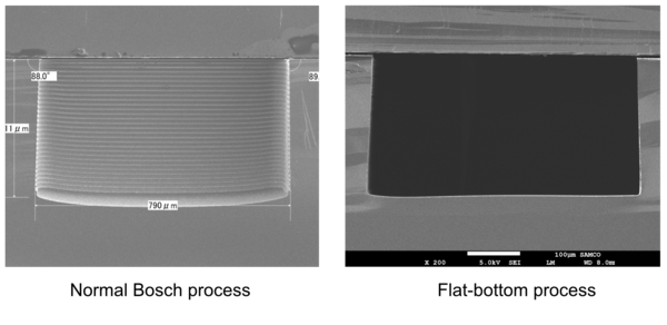
The process for suppressing the microloading effect can also be used for deep Si etching with a wide pattern as shown in Figure 7. This process suppresses not only the microloading effect, but also scallops and round shape at the bottom of trench and hole patterns. It enables anisotropic etching of patterns with widths of several hundred micrometers. However, adjusting process conditions to optimize the depth uniformity of the flat-bottom process is very challenging. Samco has a wealth of knowledge and process libraries for the flat-bottom process and is able to provide our customers with the most suitable deep Si etching processes.
Fig. 7: SEM image of the flattened bottom of the wide pattern
What the Samco Si-DRIE Can Do?
Anisotropic Silicon Deep Reactive Ion Etching process using the Bosch Process and Non-Bosch Process enables trench, hole and pillar fabrication for various device applications. These are some examples of structures fabricated using the Bosch Process. For more details, please visit the processes below.
Samco Product Portfolio for Silicon Deep Reactive Ion Etching
Our systems have industry-leading process capabilities, and the product lineup covers both R&D and production.


