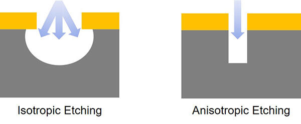
Silicon is most well-known as a semiconductor material, but because of its high mechanical strength and ease of processing, it is also commonly used in a wide variety of devices such as MEMS, optical components, micro-channel devices, and packaging. There are many methods for processing silicon, such as dry etching, wet etching, and laser processing, each of which has advantages and disadvantages that should be evaluated carefully and compared.
The processing method called Si-DRIE is a type of plasma dry etching. The etching technology cultivated for semiconductors has improved the processing of mechanical devices and has been proven to allow faster and deeper etching of features with higher aspect ratios. Among Si-DRIE techniques, there are three main process types: the Bosch process, Non-Bosch processes, and Cryogenic etching. Since silicon and fluorine atoms react very easily, processing silicon using a simple fluorine chemistry process results in an isotropic profile. Therefore, the key for increasing the verticality and aspect ratio for any of the three process types is to suppress lateral etching and develop an anisotropic process.
The Bosch process is a technique which alternates between depositing a protective film on the sidewall using a C4F8 plasma and etching the bottom of the trench or hole with SF6. The Non-Bosch process is a technique of simultaneously depositing a protective layer on the sidewall and directionally etching the bottom of the feature with ions. Cryogenic etching is a method similar to the Non-Bosch process and suppresses the chemical reaction of Si and F atoms on the sidewall by lowering the substrate temperature to that of liquid nitrogen.

The Bosch process has excellent selectivity and is capable of high aspect ratio etching and is often used for MEMS and packaging. On the other hand, the Non-Bosch process has smooth sidewalls with positive taper angle, which is useful for through-silicon vias (TSV). Additionally, the angle of the mask can be transferred into the etched material, which is often done for optical parts such as lenses. The Cryogenic etching process can achieve the selectivity of an oxide mask vs silicon equivalent to that of the Non-Bosch process. One drawback of this technique is that photo resist masks cannot be used due to the extremely low temperature of the process.
On Samco's flagship RIE-800iPB deep reactive ion etching (DRIE) system it is possible to utilize both the Bosch and Non-Bosch processes on the same system. The Bosch process enables deep and high aspect features along with extraordinary levels of selectivity to the mask. The Non-Bosch process provides deep etching with smooth sidewalls and a flexible range of taper angles. Substrate temperatures between -10°C and 20°C are controlled via liquid cooling of the bias electrode combined with electrostatic chucking (ESC) and substrate back side He gas cooling. By combining these two methods, the RIE-800iPB delivers versatile, efficient, gentle and affordable solutions for MEMS, TSV, packaging, and other applications. It's been exciting to see the continual evolution of our Si DRIE solutions as we incorporate new customer requirements into the system design.
Do you have a process challenge? Give our experienced process engineers the opportunity to meet your challenge and exceed your expectations.
What can the Samco Si-DRIE Systems Do?
Anisotropic Silicon Deep Reactive Ion Etching process using the Bosch Process and Non-Bosch Process enables trench, hole and pillar fabrication for various device applications. These are some examples of structures fabricated using the Bosch Process. For more details, please visit the processes below.
Samco Product Portfolio for Silicon Deep Reactive Ion Etching
Our systems have industry-leading process capabilities, and the product lineup covers both R&D and production.


