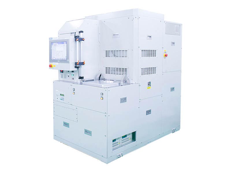
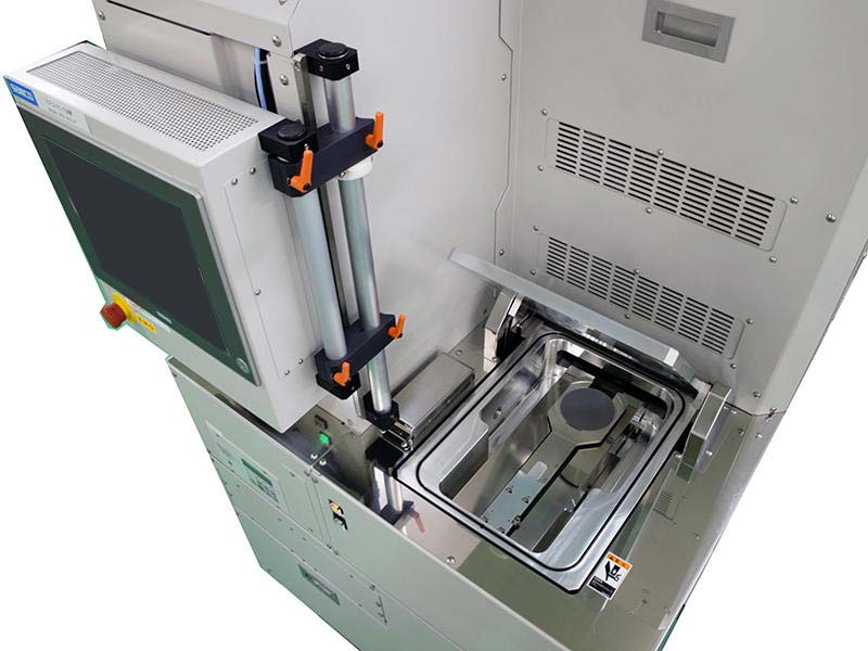
ICP-RIE Plasma Etching System RIE-400iP
GaN, GaAs, InP, & SiC
Description
The RIE-400iP load lock ICP-RIE plasma etching system utilises high-density inductively coupled plasma (ICP) to achieve precise etching. Designed for wafers up to 100 mm (4 inch), the system features an advanced ICP source, temperature-controlled electrode, and a high-flow exhaust system, all within a compact, space-saving design. This system provides reliable and exceptional process control, ensuring excellent efficiency for a wide range of etching applications, including GaN, GaAs, InP, SiC, and various other materials.
Key Features and Benefits
- Advanced ICP source enables highly uniform, high selectivity, and precise etching
- 2 kW RF power can be applied efficiently and stably
- ESC and He backside cooling for optimum temperature control
- The high flow exhaust system directly connected to the reaction chamber
- Compatible with ø2", 3", and 4" wafers
- In-situ end-pointing using interferometric and/or optical emission spectroscopic endpoint monitors
- Fast-switching gas input for ALE process as an option
Applications
- InP ridge etch for edge emitting laser
- InP DFB grating etch
- GaAs/AlGaAs mesa etch for VCSELs
- High selectivity etch of GaN/AlGaN
- GaN recess etch
- SiC/GaN trench etch for power electronics
- GaSb/InSb etch for NIR/SWIR sensors
- SiO2 and SiNx etch
- Al, Cr, Ni etch
Options
- Interferometric endpoint monitor
- Optical emission spectroscopy (OES) endpoint monitor
- Fast-switching gas line for ALE process
Papers
- Kondo, Takaaki, Yoshihiko Akazawa, and Naotaka Iwata. "Effects of p-GaN gate structures and fabrication process on performances of normally-off AlGaN/GaN high electron mobility transistors." Japanese Journal of Applied Physics 59.SA (2019): SAAD02.
- Raj, Vidur, et al. "High-efficiency solar cells from extremely low minority carrier lifetime substrates using radial junction nanowire architecture." ACS nano 13.10 (2019): 12015-12023.
- Papadogianni, Alexandra, et al. "Two-dimensional electron gas of the In 2 O 3 surface: Enhanced thermopower, electrical transport properties, and reduction by adsorbates or compensating acceptor doping." Physical Review B 102.7 (2020): 075301.
- Soo, Joshua Zheyan, et al. "Protocol for scalable top-down fabrication of InP nanopillars using a self-assembled random mask technique." STAR protocols 4.2 (2023): 102237.
- Berthold, Theresa. Gaswechselwirkungsreaktionen mit Indiumoxidschichten und deren Einfluss auf die elektronischen Oberflächeneigenschaften. Diss. Technische Universität Ilmenau, 2018.


