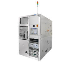
ICP-RIE Plasma Etching System RIE-230iP
Versatile loadlock system
Description
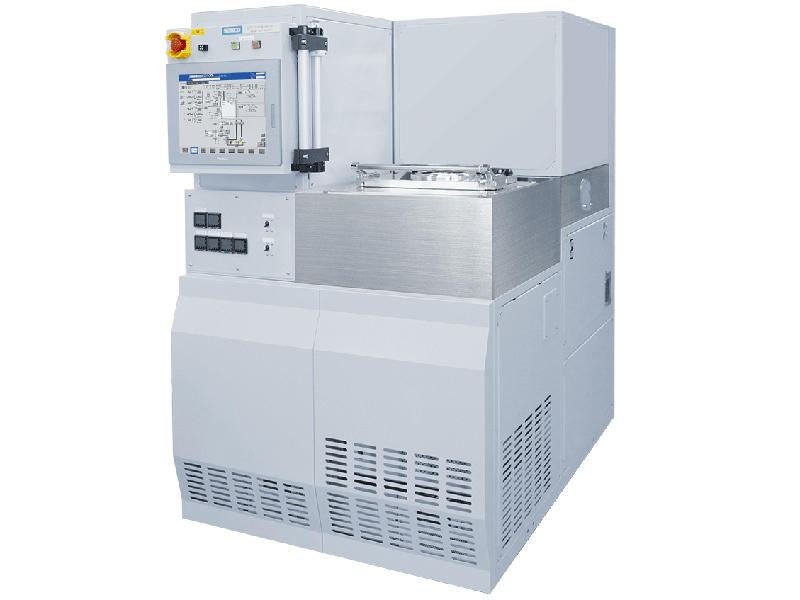
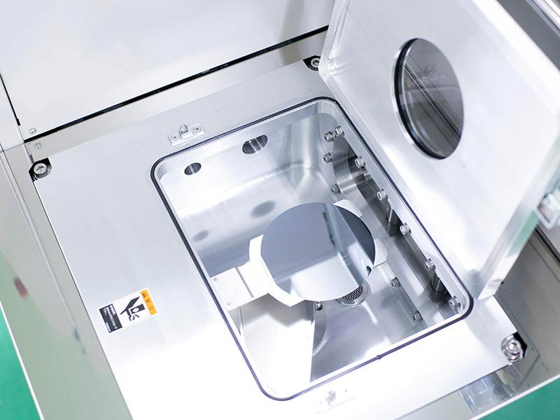
The RIE-230iP is a load-lock ICP plasma etching system that uses an inductively coupled plasma as the discharge to perform ultra-fine processing of various materials at high speed. This system efficiently generates stable, high-density plasma by employing a unique tornado-type coil electrode to enable high-precision anisotropic etching of silicon and various metal thin films and compound semiconductors. In addition, the ø230 mm carrier tray enables simultaneous processing of many compound semiconductors.
Key Features and Benefits
- Processing up to ø230 mm (ø3" x 5, ø4" x 3, ø8" x 1)
- Samco's Tornado ICP™ coil can efficiently generate stable, high-density plasma, enabling high selectivity, high accuracy and good uniformity in etching
- A symmetrical evacuation design coupled to a TMP creates an efficient flow
- An optimized gas manifolds to deliver process gas uniformity
- Optional optical/interferometric endpoint detection system enables precise etch depth control over multiple process runs
- ESC and He cooling of the stage and temperature control of the inner side wall of the reaction chamber allow etching under stable conditions
Applications
- High-precision processing of compound semiconductors such as GaN, GaAs, InP, etc.
- Processing of difficult-to-etch materials such as ferroelectrics and electrode materials.
Papers
- Tran, B. T., Hirayama, H., Maeda, N., Jo, M., Toyoda, S., & Kamata, N. (2015). Direct growth and controlled coalescence of thick AlN template on micro-circle patterned Si substrate. Scientific reports, 5(1), 1-6.
- Zhao, X., & del Alamo, J. A. (2014). Nanometer-scale vertical-sidewall reactive ion etching of InGaAs for 3-D III-V MOSFETs. IEEE Electron Device Letters, 35(5), 521-523.
- Mori, T., Yamashita, N., Kasa, H., Fukumi, K., Kintaka, K., & Nishii, J. (2009). Periodic sub-wavelength structures with large phase retardation fabricated by glass nanoimprint. Journal of the Ceramic Society of Japan, 117(1370), 1134-1137.
- Lin, J., Antoniadis, D. A., & del Alamo, J. A. (2015, May). A CMOS-compatible fabrication process for scaled self-aligned InGaAs MOSFETs. In Proc. CS MANTECH (pp. 239-242).
- Kolodziejski, L. A., & Ippen, E. P. (2008). Advanced Plasma Etching of Complex Combinations of III-V Heterostructures. MASSACHUSETTS INST OF TECH CAMBRIDGE RESEARCH LAB OF ELECTRONICS.


