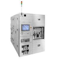
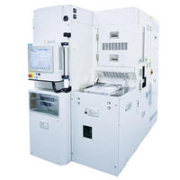
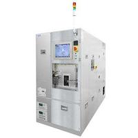
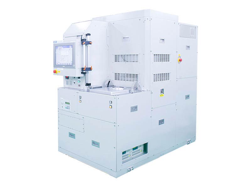
ICPエッチング装置 RIE-400iP
GaN, GaAs, InP, & SiC

概要
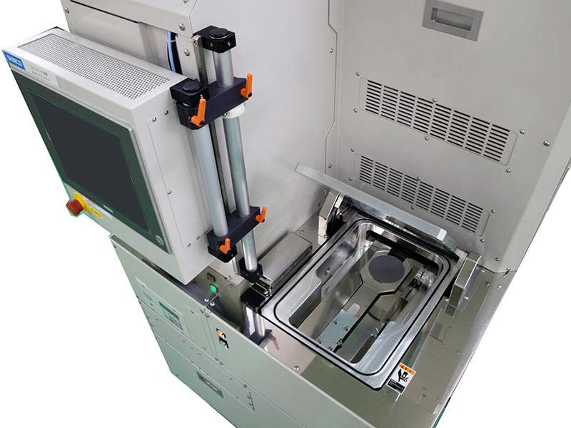
本装置は、放電に誘導結合プラズマ方式を採用したICP (Inductively Coupled Plasma) エッチング装置です。独自のICPソースであるHSTC™ (Hyper Symmetrical Tornado Coil) を搭載し、安定した高速・高均一加工を実現します。ロードロック室を備え、最大ø4インチウエハの枚葉処理に対応しており、優れたプロセス再現性を誇ります。当社は、化合物半導体や電子部品などの加工において、長年の経験と高度な技術で多様なニーズにお応えします。
特長
- ICPソース「HSTC™」により高RFパワーを効率よく安定して印加可能
- ESC(静電チャック)とHeによりウエハの安定した温度制御が可能
- 反応室直結の排気システムにより、小流量・低圧力域から大流量・高圧力域の幅広いプロセスウィンドウを実現
- ø2、3、4インチウエハの直接搬送枚葉処理が可能
- 発光分光型または干渉型のエンドポイントモニターによる終点検出が可能(オプション)
応用例
- InPのリッジ加工
- InPのグレーティング加工
- GaAs VCSELのメサ加工
- GaN/AlGaNの高選択比加工
- GaNのリセス加工
- 縦型GaNパワーデバイスのトレンチ加工
- SiC MOSFETのトレンチ加工
- SiO2、SiNの加工
- Al、Cr、Niなど金属の加工
オプション
- 干渉型エンドポイントモニター
- 発光分光型エンドポイントモニター
技術資料
論文
- Kondo, Takaaki, Yoshihiko Akazawa, and Naotaka Iwata. "Effects of p-GaN gate structures and fabrication process on performances of normally-off AlGaN/GaN high electron mobility transistors." Japanese Journal of Applied Physics 59.SA (2019): SAAD02.
- Raj, Vidur, et al. "High-efficiency solar cells from extremely low minority carrier lifetime substrates using radial junction nanowire architecture." ACS nano 13.10 (2019): 12015-12023.
- Papadogianni, Alexandra, et al. "Two-dimensional electron gas of the In2O3 surface: Enhanced thermopower, electrical transport properties, and reduction by adsorbates or compensating acceptor doping." Physical Review B 102.7 (2020): 075301.
- Soo, Joshua Zheyan, et al. "Protocol for scalable top-down fabrication of InP nanopillars using a self-assembled random mask technique." STAR protocols 4.2 (2023): 102237.
- Berthold, Theresa. Gaswechselwirkungsreaktionen mit Indiumoxidschichten und deren Einfluss auf die elektronischen Oberflächeneigenschaften. Diss. Technische Universität Ilmenau, 2018.
関連ページ
当製品以外のICPエッチング装置はこちらからご覧いただけます。